16
16
Your Cart
Large Hydrogen/Helium spectrum discharge tube 250mm - NEW
2+ shoppers have bought this
Sodium discharge tube - Very bright - NEW
17+ shoppers have bought this
 98,00
Helium-3 Isotope discharge tube 70mm - NEW
14+ shoppers have bought this
Helium-3 Isotope discharge tube 70mm - NEW
Price:
 48,00  47,04
- +
 141,12
Bromine discharge ampoule - NEW
Price:  39,90
- +
 119,70
Placeholder
1+ shoppers have bought this
 59,00
Placeholder
1+ shoppers have bought this
 62,00
PT07 Smart Radon Gas Detector - WIFI with TUYA/Smartlife App.
3+ shoppers have bought this
New! Aerogel Nanogel Granules in ampoule
1+ shoppers have bought this
 17,90
Cerium potassium phosphate glass ingot 30mm
2+ shoppers have bought this
 179,00
Nickel 2+ doped glass bead NEW!
Price:  24,90
- +
 24,90
Large Lutetium potassium phosphate glass ingot - 17mol% Lu2O3
 1 558,20
Big Tungsten Metal Sphere 1kg - 99.95% purity
1+ shoppers have bought this
 479,00
100mg high purity Rubidium Metal in mini ampoule - >99,99%
2+ shoppers have bought this
Solid Chromium Metal Sphere 30mm - 99.9% purity - ~ 100 grams
8+ shoppers have bought this
Acrylic Element cube - Ultrapure Phosphorus red P - 50mm
4+ shoppers have bought this
High pure Selenium doped Black Phosphorus 100mg
1+ shoppers have bought this
 149,00
Calculate Shipping
Shipping options will be updated during checkout.
Apply Coupon

2D – Materials, Semiconductors

2D-Materials

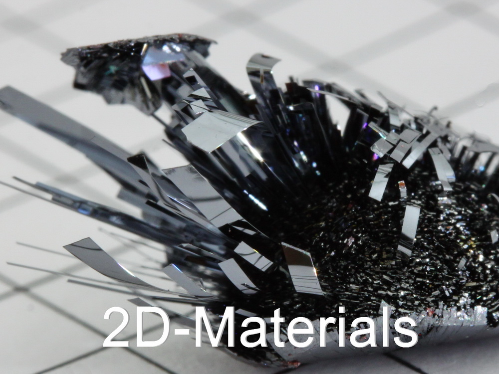
2D Materials, sometimes referred to as single layer materials, are crystalline materials consisting of a single layer of atoms. These materials have found use in applications such as photovoltaics, semiconductors, electrodes and water purification.

2D materials can generally be categorised as either 2D allotropes of various elements or compounds (consisting of two or more covalently bonding elements). The elemental 2D materials generally carry the -ene suffix in their names while the compounds have -ane or -ide suffixes. Layered combinations of different 2D materials are generally called van der Waals heterostructures.

The efficient integration of 2D functional layers with three-dimensional (3D) systems remains a significant challenge, limiting device performance and circuit design.

Some 700 2D materials have been predicted to be stable, although many remain to be synthesized. The global market for 2D materials is expected to reach US$390 million by 2025, mostly for graphene in the semiconductor, electronics, battery energy and composite materials markets.

Scroll to Top